Educational model of circular particle accelerator
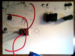
I shall tell You a story of one idea, a few sleepless nights and the love of physics. This article will be very long, because I want to explain principles and methods used in the process of making the model, share schematics, PCBs and assembly plans for everybody to benefit from them; so buckle up, prepare a bowl of popcorn and read on if You like!
One day, my fiancée got an assignment at school - She was told to prepare a presentation of some topic from the field of physics, a topic of Her choice. And it was at that moment, when an idea inspired the idea - She chose the topic of particle accelerators. And, having me - the physics and experiments enthusiast - at home, She decided to add a real experiment to enrich the presentation. And here it began - by me getting some components together and Her drawing the schematic symbols next to them. Understand - it was Her first circuit to make and the first opportunity to learn electronics.
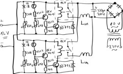
It was a fun project, for which we had a few days of time and some old electronic parts carefully acquired over a long DIY-ing period of time lying around. Back in the day, I took a tablet and created a quick draft of schematic diagram, which You can see nearby.
The idea was simple - the triggering circuit would power on a relay upon photogate beam interruption. A capacitor bank would then be discharged through the relay contacts to the coil. The photogates would be placed right at the coils, which would attract a steel ball representing a particle in a circular tube. Only for a brief moment - not to decelerate the ball, after it reaches the center of the coil. There would be two coils, hence two identical triggering circuits. The rest of the schematic is nothing more than a transformer with a bridge rectifier and another independent 12VDC power source.
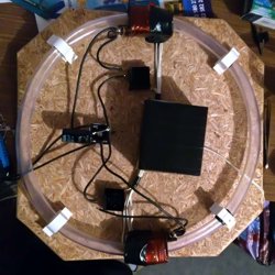
And there it was - the first quick accelerator model has been made. You can see an MDF board with a circle of plastic hose, circuit soldered on universal PCB and covered with black enclosure, two black relays and a bridge rectifier with a capacitor. Black electrical-tape-covered areas in front of the two coils are the photogates (working in the visible spectrum this time, so we had to cover them properly).
The presentation went well. The model was working and the steel ball in the hose was happily accelerated over and over again. But, after some time, another idea arised - would it be possible to make this model better? To write a final high school thesis about it's construction and educational purpose? The answer, in short, was YES!
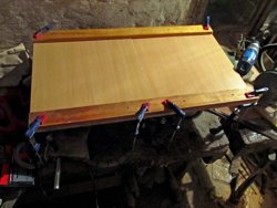
And so it began - the thesis was to have three main parts: Particle accelerator theory and history, Particle accelerators at home and schools and finally, Construction of particle accelerator educational model. She went on to write the theoretical parts and meanwhile, I assembled the base for the device. It consists of old furniture parts - in this case of two MDF pieces with surface finish screwed together. Total dimensions of base are roughly 40x80 cm. It was clear that the whole thing will not only take some space, but also weigh quite a bit...
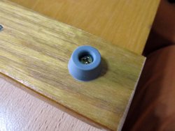
Being a massive MDF itself and having to carry substantial transformer and capacitors, casing etc., the device could certainly scratch a table when moved without care. So I decided to add four protective rubber feet to prevent damage to the furniture and to the device alike. It also makes the stability much better. I used small rubber door-stoppers and attached them with a single wood screw each. Because of the dimensions and weight, we also added two handles in the end (which are not seen on the photo here).
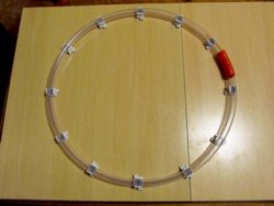
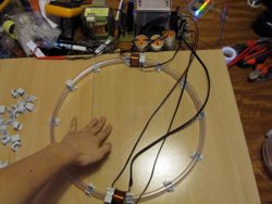
The next step was to make the accelerator circle. At first, we experimented with glass tubes - I sawed off the ends of the circular fluorescent tube, removed the luminophore and tried to make a sillicone piece to close the gap in the glass. It was a difficult process, because a thin round glass tube likes to crack and break... a lot. But the hardest part was to make the piece to close the gap without having a rough transition. We discarded the idea also because a steel ball hitting the glass tube walls... doesn't sound right. So we chose transparent PVC hose and attached it to the base using two-part plastic cable holders.
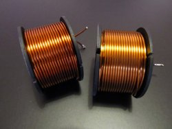
Having the tube in place, we needed to make the coils. It was necessary for them to withstand great current spikes (in the order of hundreds of amps) and to create strong enough magnetic fields. Through some calculations and experimentation we determined that the optimal number of turns is about 60 wound with 1mm enamelled copper wire. Coils have three layers, about 20 turns each. Their dimensions are roughly 2 cm of length and 2,5 cm of diameter. Because the wire is thick, we used back-and-forth style of winding.
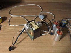
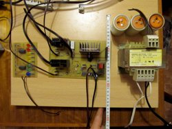
Now for the power parts - we obtained a 400 to 230 VAC transformer with tapped primary winding. My intention was to use it for both purposes - powering the low voltage parts (as autotransformer) and the power parts (charging the capacitor bank from secondary) from 230 VAC line. And so it happened - you can see the test setup with some rectifiers and capacitor bank. The transofmer has about 160VA power rating (which later turned out to be way less than comfortable...) and about 135 VAC effective output. It is obligatory to put a warning here - the capacitor bank with capacity of 1,6 mF charged to about 180 V IS DEADLY. It holds about 26 J of energy with voltage certainly high enough to harm or even kill You. Know what you are doing or do not do at all!

For the capacitor bank, I used three electrolytic capacitors with 4,7 mF / 63 V rating in series. It got me about 1,6 mF of capacity and a maximum voltage of about 189 V. A fun picture of some testing can be seen nearby - fast discharge of the capacitor bank results in a spectacular spark and some molten metal droplets flying around. Wires connecting the capacitors have to be a little hefty too - I used 2mm stranded copped cables to be sure they can handle the current spikes without heating.
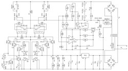
Let's get to the main part of this article - you can see the schematic diagram nearby. Open it in the next window and read on if You want to know what I did there... I will divide the explanation into three parts - 1) Power sources, 2) Triggering circuits and 3) Capacitor charge regulators.
I will make the first part about power sources short - there are two of them. One for the power part (charging the capacitor bank), one for powering the low-voltage circuits. The first part is powered from main transformer's secondary winding. The voltage here rises roughly up to 185 VDC after rectification by B1. However, it does not go anywhere else unless SCR1 is on - and I'll speak about it later on, because it is a fundamental part of regulation circuit. Only next part here is R3 and D1, which signal that the high voltage part is powered. The bottom part of the schematic shows a classic use of bridge rectifier B2 followed by 7812 stabilizer with filtration capacitors around it. R19 and D9 are used to signal that low-voltage part is powered. Last words about power source part: There is a fuse in the primary of the Tr1. To make it at least a little safe. There also are main power switch S1 and high-voltage part switch S2. This was done to ensure that everything is wokring before the user charges the capacitor bank. Let's move on to the triggering circuit.
I shall describe only one of two identical triggering circuits, because each coil has it's own independent triggering, only some parts are shared by both. The principle is fairly obvious - take the right triggering circuit for coil L1: Infrared LED D10 shines to the IR phototransistor T4, which brings positive voltage to the base of T8, hence closing it. At this moment, (almost) no current flows to the base of T10, the same applies to T2. But as soon as the beam is interrupted by passing ball, phototransistor T4 sharply rises it's resistance, so Pot3 can pull the voltage on the base of T8 low enough to open it. Now the current is further amplified by T10 and led to the base of T2. At the same moment, C11 discharges (producing a little delay) and T2 powers the relay Rel1 on. The ball passes, transistors T8 and T10 close again, but T2 stays on for the next while, because C11 is charging through it's base. This is very important - it lengthens the pulse so it is enough to trigger the relay. Without it, the pulse duration would not be enough for the relay to switch it's contacts. There also is a protection diode D6 in parallel to the relay coil to prevent the voltage spikes from returning to the transistors. And here the magic comes - the relay is not here to transfer the capacitor bank energy to the accelerator coils! We've tried it... did not end well for the relay contacts. The currents are just too large for them to handle. So, after some experimentation with different switching methods (and burning a few power transistors...) I decided to use a thyristor SCR1 as a power switch. But it's gate requires a VERY sharp pulse to turn on - so sharp that it was unreliable with transistors and I used a relay instead. Finally, there is another protection diode D2, which absorbs the induced voltage spikes from accelerator coils. This solution works the best - nothing fries, nothing melts together, nothing skips a ball passing the photogate... The last component here is diode D3, which brings the positive voltage to the common lead of the relay switch. And that is all - the ball passes through the IR photogate, interrupts the beam, amplifier amplifies and lenghtens the spike, powers the relay, it switches the thyristor, which leads energy from the capacitor bank to the accelerator coil. Capacitor bank discharges, thyristor returns to non-conductive state and the cycle repeats with each revolution.
And here the black, smoky, magic comes - the capacitor bank voltage regulation circuit. The part I burned a few more power transistors on... I realized I have to discharge the capacitor bank fully with each trigger. That is the nature of thyristor - I wanted to turn it off in the simplest manner, by stopping the current flow between anode and cathode. So I needed to wait for the capacitor bank to fully discharge. But... how to regulate the amount of energy fired during one trigger event? The answer was obvious - I have to charge the capacitor bank to variable voltage. Voltage I have to have a way of controlling. And here lies the reason of my sleepless nights! I had to be able to set up voltage from almost 0 V to almost 200 V. Which proved to be a little bit challenging, because most of the active components could not handle that range of voltage. I needed a power component capable of running a few amps through at almost 200 V and stopping the current flow on command (when the desired capacitor bank voltage is reached). I tried power BJTs and MOSFETs, but every time I ended up with a fried transistor. The reason (which I discovered way too late...)? Overvoltage at base/gate. Every time. I just was not able to make the voltage to stay in certain boundaries. And then it hit me. Let's walk You through the solution I came up with.
It may appear that negative rails of both rectifiers are connected, so the circuit does have a common ground. And it is true. Just... it does NOT apply to the branch of circuit after the thyristor SCR1. Positive lead of the capacitor bank is always at the maximum voltage in relation to common ground (which spikes at about 185 V). But it's negative leads are - surprise - on the same potential, when the bank is discharged. When SCR1 opens, the bank charges. Bank's negative lead then gradually lowers it's potential and the more the capacitor bank is charged, the lower is it's negative lead's potential in relation to the common ground. At full charge, negative lead has almost the ground potential. It means that the lower negative lead voltage, the higher the capacitor bank charge. And this fact is used to regulate the bank voltage - I added the divider consisting of R6 and R5, which drops the voltage to about two fifths (from 0-185 V to 0-70 V). From the middle of this divider, there is another one consisting of R7, R8 and Pot1. Resistance value of the second divider is an order higher than the first divider's value to ensure it does not affect it too much. R7 and R8 limit certain minimal and maximal values the user can set the voltage to by turning the potentiometer. Resistor R9 is added to change the shape of the potentiometer response curve to make the voltage setting a little more linear with the position of the potentiometer (without it, the voltage increment with position change would be close to exponential). And here we get to the LM2903 comparator - potentiometer leads the signal to it's inverting input. The non-inverting input is kept at 3 V thanks to D8 and R16. What does it mean? The comparator will do anything to keep the inverting input at the same 3 V. And it does it through it's output wired to the base of T1 PNP transistor, which, when opened, turns on the SCR1, which charges the capacitor bank. Let's now inspect the circiut.
If the capacitor bank is not charged, it's negative lead is at the voltage close to 185 V, hence there is about 70 V in the middle of the first divider (R6, R5). If the potentiometer wiper is somewhere in the middle, the voltage on it's middle terminal would be about 35 V. Which is way more than 3 V on the non-inverting input of the comparator. So, there is 0 V on the output of the comparator - this means that the current flows from the T1's emitter to it's base, through R15 and the active open-collector comparator output to the ground. This means T1 is open, so the SCR1 is in conductive state. The capacitor bank is charging, the voltage on it is rising. This means that the negative lead of the capacitor bank is lowering it's voltage in relation to the common ground. Let's now imagine that the voltage on the capacitor bank is high, almost at the maximum. It means that the negative lead is at almost 0 V. There must be about 0 V in the middle of the first divider (R6, R5), hence on the wiper of Pot1, hence on the inverting input of the comparator. And there still are the same 3 V on the non-inverting input. What does that mean? Voltage on the non-inverting input is higher than voltage on the inverting input, so the open-collector output is closed. No current flows through it. It leaves T1 with positive voltage appearing on it's base through R14. T1 is closed, hence SCR1 is closed - it means that the capacitor bank is not being charged. And this happens as soon as the voltage on the inverting input drops under 3 V. Et voilá - here we have a way to regulate 0-200 V!
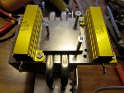
Of course, there are a few more tricky parts - and that is why there are a tiny bit more components used. Remember the note about insufficient transformer power? Here it shines through - I had to add the two power resistors to limit the charging current, because otherwise the secondary winding would melt itself after a minute of run. It was no easy task, because running amps at hundreds of volts requires hundreds of watts... I chose two metal-encased 100 Ohm / 50 W resistors for this job. I had to modify CPU heatsink by cutting a few threads in it for the screws to hold the resistors tightly and cool them down. You can see them mounted on the picture. Another three threads were cut for the screws holding the heatsink at the PCB. I also added a tiny temperature-control circuit with thermistor Rt1, trimmer Pot5, T7, T6 and a CPU fan M1. It's principle is fairly easy tp understand - as soon as the thermistor resistance drops under a certain value (which happens when the temperature rises), T7 opens, which opens T6 and it turns the fan on. The fact that the thermistor is attached to the heatsink provides the circuit with a kind of hystheresis (more precisely a delay) - the fan always stays on until the resistor temperature drops a bit. This circuit was not that necessary indeed - the device cannot be left running for more than a few minutes anyway because of the transformer secondary overheating, but hey - a few minutes are better than under a minute. The steps taken? Charging current limiting resistors, fan cooling down the transformer, temperature-controlling circuit and a fan cooling down the resistors. Was it worth it? Well, I believe so - without these measures, the probability of a user frying the transformer would be much higher. And with them, it is enough to obtain a more powerful power source and the device would run on and on. Next trick is in the R3+D1 - they are there not only to signal that the high-voltage part is powered, but also to slowly discharge the capacitor bank when not in use. The charged capacitor bank could be deadly even long after the device was running - so I added this simple solution to discharge it safely. There also are a few capacitors with capacities in the order of hundreds of nanofarads - their purpose is to make sensitive circuits more stable (namely comparator and stabilizer). You could notice a few trimmers around the diagram - Pot3 and Pot4 set the photogate trigger level, which is very important for them to work correctly. Pot5 sets the heatsink temperature at which the fan turns on. And the last one - Pot2 - sets the sensitivity of bar graph capacitor bank voltage indicator (further discussed bellow).
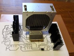
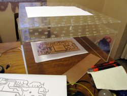
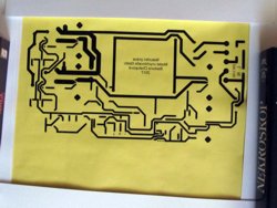
The CPU heatsink was not alone, because there were more components generating non-trivial amounts of heat - such as 7812 providing power for all the low-voltage circuits and fans and the SCRs providing control over the large currents. All those heatsinks had to fit on the PCB, so I measured them, drafted the PCB layout and printed it out to test it before making the PCB. You can see how it turned out on the nearby image. The TO220 heatsinks are classic black surface aluminum heatsinks with dimensions roughly 50x40x20 mm. Thermal grease was applied to all the components and there was no problem with cooling.
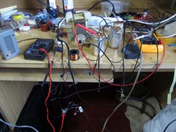
Everything at my workskop begins as a dangerous gamble with electricity held in my hands - as you can see on the image nearby. After all the experimenting with the final regulation circuit idea, some measurements and calculations were made to be sure everything works before I make the PCB. I also tested the trigger circuits - some dents from the steel ball in my ceiling still remind me of the success back in the day. Fun fact: notice the lightbulb on the table. It is the best way of dicharging the high voltage capacitor banks to be sure they don't kill somebody after you leave them unattended for a nanosecond.
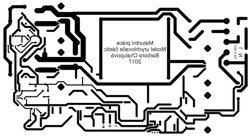
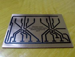
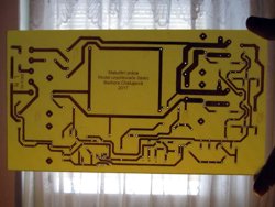
The final PCB pattern, which you can download from the image nearby, should be 238 mm wide (left-most trace to right-most trace, add a few mm as a boundary). Trace width is a compromise between space and current requirements, but practical experience show that it is sufficient at least. The text in the middle of the area bellow the big heatsink says that this PCB is a part of final thesis of my fiancée, Barbora Chalupová, so You can omit this. Because of the fact that the PCB was to be made by myself, I added some necessary texts to the PCB layer, but if You were to have it manufactured, it would go to the silk layer.
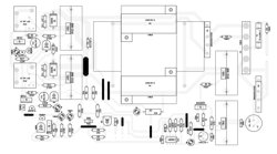
The next image nearby depicts the component layout. The only change from the schematic is the capacitor bank connection - it is shown as a single C1, but in fact, two thick 2mm stranded copper cables go there to connect to the bank placed elsewhere. The same applies to Pot1, which will be mounted in the front panel. The fuse holder is a simple cheap two-part metal type, which is economical and allows a quick fuse change.
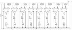
Next pleasant duty was to design a visually appealing voltage indicator. This task was taken by a simple comparator bargraph described in the previous article (unfortunately, not available in english yet), just altered a little bit to work with 8 LEDs instead of 12. Let me briefly explain the principle here because of the language barrier.
If we take it from the end - the LED connected to the open-collector output of the comparator lights up when the output is LOW. This demands the voltage on the inverting output to be higher than the voltage on the non-inverting input. All the non-inverting inputs are connected to the wiper of trimmer Pot2 from the main board. Let's recap: the higher the charge on the capacitor bank, the lower the voltage here. The inverting inputs of the comparators are connected to the resistor cascade R38 - R29. There is 1/9 of supply voltage on the first inverting input, 2/9 on the second, etc. and the last inverting input is at 8/9 of the supply voltage. So, if the input voltage from Pot2 is, say, 10 V (the capacitor bank is mildly charged), only the first LED (D19) will be lit, because voltage on it's comparator's inverting input is about 10,7 V, which is higher than 10 V on non-inverting input. But for the second comparator, there is 9,3 V on the inverting input, hence the voltage on it's non-inverting input is higher, so it's output is turned off (remember - it is open-collector output after all). This applies to all the other comparators. If the capacitor bank charges more, say to the half of the maximum voltage, the voltage on the Pot2 wiper could be around 5 V. In this case, first five LEDs will be lit (D19 - D15), because voltage at IC1D's inputs are 5 V at non-inverting and 5,3 V on the inverting input - so the LED at the output is lit. For IC1C, the voltages are 5 V on non-inverting input and 4 V on inverting input, so the output is turned off. Last lit LED is hence D15.
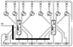
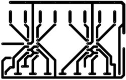
The bar graph PCB should be 100 mm wide (again - trace to trace, add a few mm as a boundary). 10mm LEDs were used for the effect - they just look great. The boards are connected by three cables - two power and one signal cable. You can see all of the connection points marked on both main PCB and bar graph PCB. You can also notice two top layer paths designated on the component layout picture - which is vastly unnecessary, I used two pieces of copper wire to make these connections and one-layer PCB. ICs of my choice were LM239 quad comparators because of their price and availability - You can substitute them for any other type with equivalent pinout.
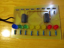
You can see the color composition of the LEDs - the first one to light up is the blue one (it is possible to see the PCB pattern orientation through). One last note - since the comparators are very sensitive circuits, there is another 100 nanofarad capacitor (C4) on the wiper of Pot2 - it is necessary for the stability of displayed number of LEDs. After some experince, I put the ICs to the sockets - they tend to fail, when You hard-solder them into PCB... and I don't need to tell You, what a joy it is to have to replace a component in DIP14 package, when soldered to the board.
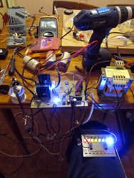
The time has come to put all the ideas to the test - and do some final tweaking. The image nearby depicts the test process. Multimeter display shows the current capacitor bank voltage, the bar graph shows all the LEDs lit up. You can notice a different board on the table - that was the first version of the PCB, which had to be tweaked a little bit - during those sleepless nights. Even now there is board version 2.2 in the model, but the PCB patterns provided here are version 3.0. The time-pressure just produces bugs. It happens. Get over it.
Anyway, the test was successful. I could do some measurements and modify a few component values. The accelerator worked at this moment - not perfectly yet, but it was the first spark of hope that we will get this done on time in the end.
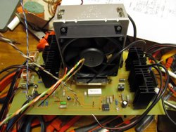
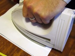
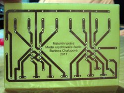
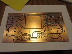
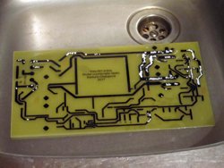
When everything necessary for the device to work was done and reflected in the PCB pattern, I made the PCB using the toner-transfer method described in the previous article. It looks a little bit like an octopus on the photo nearby - that is because it has many components that have to be elsewhere: Pot1 to set up the voltage, D10 and D11 with T4 and T5 at the coils, fan M1 and thermistor Rt1 at the heatsink, coils, capacitor bank, transformer, switches and the bar graph board. See? Many cables.
What followed was a series of finishing tasks - screw everything together, make an acrylic casing, solder everything together etc. You can see how it turned out in the video:
Some final words: You could get the impression that I've done all the work and my Significant other presented is as Hers. But that would be dead wrong - She participated in almost every manual work step - she soldered, screwed, cut, even tried flame-polishing of acrylic cuts, etc. and wrote a thesis about all this. The only part She (understandably) could not get Her hands into was the circuit designing. She had next to no experience in the field of electronics and there were quite a few challenges to overcome. But in the end, everything worked fine - She understood the principles afterwards, learned a bit of electronics, successfully graduated and the model stays at school to educate next generations of students. Happy end, right? :-) And now, after more than a year, I finally got myself to write this article so anybody can get some inspiration here and experiment on. For the love of physics! :-)
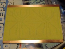
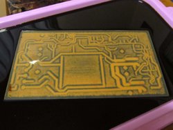
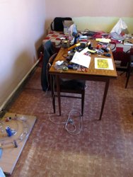
Let's finish with some more photos of the making process, this time without a commentary (because there was more than enough of that already :-) )...

|
WARNING: The author holds no responsibility for the possible damage to health or property done by attempting to recreate the devices described here or their parts! Use common sense and be VERY careful!
Your Sima
Discussion:
6.12.2022, 15:58 |
|
| - - - - - - - - - - - - - - - - - - - - - - - - - - - - - - - - - - - - - - - - - - - - - - - - - - - - - - - - - - - - - - - | |
6.12.2022, 15:58 |
|
| - - - - - - - - - - - - - - - - - - - - - - - - - - - - - - - - - - - - - - - - - - - - - - - - - - - - - - - - - - - - - - - | |
6.12.2022, 15:58 |
|
| - - - - - - - - - - - - - - - - - - - - - - - - - - - - - - - - - - - - - - - - - - - - - - - - - - - - - - - - - - - - - - - | |
6.12.2022, 15:58 |
|
| - - - - - - - - - - - - - - - - - - - - - - - - - - - - - - - - - - - - - - - - - - - - - - - - - - - - - - - - - - - - - - - | |
6.12.2022, 15:58 |
|
| - - - - - - - - - - - - - - - - - - - - - - - - - - - - - - - - - - - - - - - - - - - - - - - - - - - - - - - - - - - - - - - | |
| Aryan 24.9.2020, 13:24 |
Can I get the parts from u and everything what u used to make it |
| - - - - - - - - - - - - - - - - - - - - - - - - - - - - - - - - - - - - - - - - - - - - - - - - - - - - - - - - - - - - - - - | |
3.1.2020, 11:56 |
|
| - - - - - - - - - - - - - - - - - - - - - - - - - - - - - - - - - - - - - - - - - - - - - - - - - - - - - - - - - - - - - - - | |
2.10.2019, 11:7 |
What power source did you use for this project? |
| - - - - - - - - - - - - - - - - - - - - - - - - - - - - - - - - - - - - - - - - - - - - - - - - - - - - - - - - - - - - - - - | |
| Apu 26.9.2019, 11:11 |
Can it makes 220v to 1500? |
| - - - - - - - - - - - - - - - - - - - - - - - - - - - - - - - - - - - - - - - - - - - - - - - - - - - - - - - - - - - - - - - | |
| Apu 26.9.2019, 11:9 |
Can it make 220v to 1500v |
| - - - - - - - - - - - - - - - - - - - - - - - - - - - - - - - - - - - - - - - - - - - - - - - - - - - - - - - - - - - - - - - | |
| Joe 31.7.2019, 6:47 |
English Hello, I have a question for the build of the particle accelerator, can i use a 330 watt power supply along with 2 coils and a tube, I am trying to create element 115 Moscovium. Czech ahoj, mám otázku pro sestavení urychlovače částic, mohu použít zdroj energie 330 W spolu se 2 cívkami a trubicí, snažím se vytvořit prvek 115 Moscovium. |
| - - - - - - - - - - - - - - - - - - - - - - - - - - - - - - - - - - - - - - - - - - - - - - - - - - - - - - - - - - - - - - - | |
| Joe 31.7.2019, 6:34 |
what do i need to make one of these |
| - - - - - - - - - - - - - - - - - - - - - - - - - - - - - - - - - - - - - - - - - - - - - - - - - - - - - - - - - - - - - - - | |


